Toy Siren Circuit Diagram

This simple Toy Siren circuit for hobbyist and student who game liker, this is a very simple Toy Siren circuit,  This Toy Siren circuit can be built small enough to frt inside a toy. The Toy Siren circuit consists of a relaxation oscillator utilizing one uni-junction transistor (2N2646, MU10, TIS43). R2 and C2 determine the frequency of the tone. 

 Simple Toy Siren Circuit Diagram

 Simple Toy Siren Circuit Diagram
Pushing the button, SW1 charges up the capacitor and the potential at the junction of R2 and C2 rises, causing an upswing in the frequency of oscillation. On releasing the push-button the charge on C2 will drop slowly with a proportional reduction in the frequency of oscillation. Manual operation of the button at intervals of approximately 2 seconds will produce a siren sound.

Sourced By: Circuitsstream

  • Digg
  • Del.icio.us
  • StumbleUpon
  • Reddit
  • RSS

Electronic Music Maker Circuit Diagram

Build a Simple Electronic Music Maker Circuit Diagram. This electronic music maker uses an astable oscillator circuit that is controlled by a photocell. The light falling on the photo cell controls the tone. By mounting the circuit in a box, you can control light-reading PCI with your hand.

Simple Electronic Music Maker Circuit Diagram

Simple Electronic Music Maker Circuit Diagram
Best Blogger Tips

Sourced By: Circuitsstream

  • Digg
  • Del.icio.us
  • StumbleUpon
  • Reddit
  • RSS

Holiday Lighting Sequencer Circuit Diagram

Flasher bulbs use a bi-metallic strip which interrupts the series circuit when the lamp becomes hot.. This is a Best Holiday Lighting Sequencer Circuit Diagram. This is Integrated circuit Ul (a 555 oscillator/timer) is wired as a conventional pulse generator. The frequency of the pulse generator is controlled by potentiometer Rll. Resistor R2 puts a reasonable limit on the highest speed attainable. The output of the pulse generator is fed to the common clock input of U2, a 74C175 quad D-type flip-flop. 

 Best Holiday Lighting Sequencer Circuit Diagram

  Best Holiday Lighting Sequencer Circuit Diagram
Each flip-flop is configured so that its Q output is coupled to the D input of the subsequent flip-flop. Information on the D input of each flip-flop is transferred to the Q (and Q) outputs on the leading edge of each clock pulse. Switch S2 allows you to invert the information on the D input of the first flip-flop at any time during the cycle. This allows you to create a number of different sequences, which are determined by the state of the CQ output at the time of the switching. 
However, if S2 is switched to position while all outputs are high or all are low (which seldom occurs), the sequence stops and the outputs remain either all on or all off. If that happens, you only need to switch back to position A for at least one pulse duration, then back to position again. Likewise, S2 should be in position A (pin 4 connected to pin 14) each time the power is turned on. This is because the data on pin 4 must be a logic 1 in order to start a sequence; otherwise all outputs remain at logic 0, regardless of the clock pulses. Each output of the sequencing circuit is connected to an MOC3010 opto isolator/coupler (U3 through U6), which contains an infrared-emitting diode with an infrared-sensitive diac (triac driver or trigger) in close proximity. The diac triggers the triac, which carries the 117-volts ac. 
Each time that the infrared- emitting diode receives a logic 1, it turns on and causes the diac to conduct. With the opto isolator/coupler`s internal diac conducting, the triac turns on, and power is supplied to whatever load is plugged into the corresponding ac socket. So, the sequencing circuit and the 117-V ac outputs are optically coupled and are effectively isolated from each other. Power for the sequencing circuit is provided by a 6.3-V miniature transformer. The output of the transformer is rectified by a four-diode bridge circuit, the output of which is filtered by CI (1000- electrolytic capacitor). Capacitor C3 is added at the supply pin of IJ2 to suppress transients. Sourced By: Circuitsstream

  • Digg
  • Del.icio.us
  • StumbleUpon
  • Reddit
  • RSS

One Condition Trimming Circuit Diagram

One Condition Trimming Circuit Diagram. This relatively simple, inexpensive circuit requiring one trimming operation can multiply or divide with a consistent accuracy of greater than 1 part in 1,000. An inexpensive CMOS version of standard 555 timer chip T, in conjunction with low-drift LMll error amplifier A3, an inexpensive analog chopper switch SW, form a unique voltage-to-duty-cycle converter to produce the difficult transfer function necessary for accurate conversion. Read: Use 555 Build Spaceship Alarm

 One Condition Trimming Circuit Diagram

 One Condition Trimming Circuit Diagram
An unknown multiplicand voltage applied to the A3 error op amp circuit`s Y input controls the duty cycle of the timer through its pin 5 modulation input. The network between the sink-and-source output of the timer, pin 3, and the state trigger inputs, pins 2 and 6, cause the timer to oscillate. An error feedback signal from the timer`s discharge output, pin 7, represents the duty cycle. Integrating this duty-cycle signal with voltage reference REF representing full scale, and applying the result to the inverting input of A3, closes the feedback loop and insures high accuracy. Read: Rf Probe Circuit Diagram For vtvm
Multiplier X feeds into another LMll op amp, A1, which acts as a input buffer and scaler. A third LMll, A2, filters and buffers the Z output. Between A1 and A2, the timer`s duty-cycle output modulates the analog switches of a CD4066 to achieve the desired multiplier output. To perform division instead of multiplication, reconfigure the op amp A1 circuit with the use of jumpers. Amplifier A2 isn`t required in the division configuration. To calibrate the circuit, connect the X andY inputs together and apply 10 V. Read: DC to AC Inverter by IC 555
Then adjust the 10-turn span potentiometer to achieve a 10-V output at Z for multiplication, or 1 V for the division configuration. Also check for zero output at a zero multiplier input. The circuit is scaled for 0 -10 V inputs and outputs with a small overrage capability, but other scalings are possible. Star grounding or a heavy ground bus should be used to reduce offset problems that are unavoidable in this design. Sourced By : Circuitsstream

  • Digg
  • Del.icio.us
  • StumbleUpon
  • Reddit
  • RSS

Tactful Triac Controller Circuit Diagram

Simple Tactful Triac Controller Circuit Diagram. This is the sensitive triac circuit in this circuit the single transistor connected between the capacitor and the common side of the ac line allows a logic-level signal to control this triac power circuit. Resistor R2 prevents false triggering of the triac by the trickle current through the diac.

Simple Tactful Triac Controller Circuit Diagram


Simple Tactful Triac Controller Circuit Diagram

Sourced By: Circuitsstream

  • Digg
  • Del.icio.us
  • StumbleUpon
  • Reddit
  • RSS

Audio Controlled Mains Switch Circuit Diagram

This is a simple Audio Controlled Mains Switch Circuit Diagram. Simple but very forkful project for audio liker circuit. This circuit will switch off the line supply to audio or video equipment if there has been no input signal for about 2 seconds. SI provides manual operation and S2 acts as a reset. This circuit allows for time to change a tape or compact disc.About 50 mV of audio signal is necessary. Read:  Solid-State Switch For Dc-Operated Gadgets


Audio Controlled Mains Switch Circuit Diagram


Build a Audio Controlled Mains Switch Circuit Diagram


Sourced By : Circuitsstream

  • Digg
  • Del.icio.us
  • StumbleUpon
  • Reddit
  • RSS

Build a 12V 7.2Ah SMF Battery Charger Circuit Diagram

Build a 12V 7.2Ah SMF Battery Charger Circuit Diagram. The LM317 is an adjustable three-terminal positive-voltage regulator capable of supplying more than 1.5A over an output-voltage range of 1.25 V to 37 V. It is exceptionally easy to use and requires only two external resistors, R2’ and R2” (R2= R2’+ R2”) to set the output voltage. Furthermore, both line and load regulation is better than standard fixed regulators. In addition to having higher performance than fixed regulators, this device includes on-chip current limiting thermal overload protection, and safe-operating-area protection. All overload protection remains fully functional, even if the ADJUST terminal is disconnected. By connecting a fixed resistor, R1 the ADJUST and OUTPUT terminals, the LM317 can function as a precision current regulator. An optional output capacitor can be added to improve transient response.

Schematic Diagram using LM317


The ADJUST terminal can be bypassed to achieve very high ripple-rejection ratios, which are difficult to achieve with standard three-terminal regulators. A capacitor of small value should be connected across the input pin of LM317 and ground, particularly if the regulator is not in close proximity to the power-supply filter capacitor.

Please note that the output can go no lower than 1.25 Volts.The Input voltage must be about 3 Volts above the desired Output Voltage. So input voltage should be around 18V.So a transformer with the secondary voltage of 17 V is used.

Determining the Values

Vo is calculated by following formula ,  Vo = Vref * ( 1 + R2/R1 )
Where Vo is the voltage drop across the output i.e voltage applied to the charge the battery.

Here  Vref = 1.25.Making R1 a standard value, like 220 Ohms sets the current through R2 as well. Now all we have to do is select the value of R2 to give us a voltage drop of our desired V OUT, minus the 1.25 Volts across R1.

So for Vomaximum=15 v and Vominimum=12 v we get respective values of R2minimum=1K8  and  R2maximum=2K3 which we will get by keeping R2’=1k8  and R2”=500 Ohms (variable).

The most commonly used OPAMPS are 741 and 324. IC741 is used in close loop configuration and LM324 in open loop configuration. i.e. LM324 mainly used as comparator while 741 for amplification,addition etc

LM317 regulates the Output at 1.25 Volts above the Reference pin. Knowing this the value of this resistor sets the current through both resistors. The current drawn by the Reference pin is small and can be ignored as long as the current through the resistors is around 1 mA to 10 mA.

Testing your Circuit

Output voltage can be varied and obtained as wanted(between 12v and 15v,minimum and maximum charging voltages. Observed voltage values at INPUT ,OUTPUT and ADJUST pins is shown in table.While testing take enough precaution as not to short OUTPUT and ADJUST pins as it may damage the transistor BC 547,whose collector is connected to adjustment pin.

ADJUSTOUTPUTINPUTVref
13.7 V12.47 V15.01 V1.23

The difference between voltage at output pin and adjustment pin is 1.23 (~1.25) which is the reference voltage Vref. Current rating of battery to be charged 7.2 Ah 12v, short circuit current Isc = 720mA .Using multi-meter check the short circuit current.If the Isc shows a different value than expected,it can be changed by increasing or decreasing the load connected between the emitter of the transistor T1 and ground.

Working of Charger Circuit

The circuit uses two LEDs as indicators; one for signaling charging ON condition,and the other as an indicator , when charging voltage falls below  its terminal voltage (~12 volts). Terminal voltage can be adjusted by adjusting the 1k Trimpot. The output voltage range can be adjusted by 500 ohm Trimpot. LM324 is used in comparator circuit,after the rectifier circuit. Comparator will compare the voltage levels,and if the output voltage is less than the charging voltage,the voltage across the red LED will go high thus indicating drop in charging voltage.

Diode Protection for LM317T

If the battery is connected to the charger but unplugged from the power source, you end up with the input voltage of the circuit disconnected while the output voltage is still present. Some regulators can be damaged by this, and thus diodes are put into the circuit to protect them.

Applications

SMF batteries or VRLA batteries (valve-regulated lead-acid battery) are made in an eco-friendly, ISO Certified & modern plant with a large manufacturing capacity and are being sold worldwide. There is a wide range available to suit all applications of standby power requirement’s, for example:
  1. UPS (Uninterrupted power supply)
  2.  Inverter and Emergency Lights
  3. Telecommunication equipment
  4.  Fire Alarm & Security Systems
  5.  Railway Signaling
  6. Electronic Attendance & Cash Registers
  7. Solar Lanterns and Systems,
etc. come in factory charged conditions and have a high shelf life thereby requiring longer time intervals between recharging of batteries in stock.  Source : Link

  • Digg
  • Del.icio.us
  • StumbleUpon
  • Reddit
  • RSS

Audio Milli Volt Meter Circuit Diagram

Build a simple audio Milli volt meter circuit diagram. This Audio Milli Volt Meter Circuit has a flat response from 8Hz to 50 kHz at -3 db on tbe 10-mV range. The upper limit remains the same on tbe less sensitive ranges, but the lower frequency limit covers under 1 Hz.

Simple Audio Milli Volt Meter Circuit Diagram

Simple Audio Milli Volt Meter Circuit Diagram


Sourced By : http://circuitsdiagram-lab.blogspot.com/2013/11/simple-audio-milli-volt-meter-circuit.html

  • Digg
  • Del.icio.us
  • StumbleUpon
  • Reddit
  • RSS

Crystal Controlled Reflection Oscillator Circuit Diagram

How to build a Crystal-controlled-reflection-oscillator circuit diagram . This is a simple crystal controlled reflection oscillator circuit, this unit is easily tunable and stable, consumes little power, and costs less than other types of oscillators tlmt operate at the same frequencies. This unusual combination of features is made possible by a design concept that includes operation of the transistor well beyond the 3 dB frequency of its current-versus- frequency curve. 

 Crystal Controlled Reflection Oscillator Circuit Diagram

Crystal Controlled Reflection Oscillator Circuit Diagram
The concept takes advantage of newly available crystals that resonate at frequencies up to about 1 GHz.The emitter of transistor Q is connected with variable capacitor Cl and series-resonant crystal X. The emitter is also connected to ground through bias resistor Rl. The base is connected to the parallel combination of inductor L and capacitor C3 through DE-blocking capacitor and C4 and is forward biased with respect to the emitter by resistors R3 and R4. 
Impedance Z could be the 220-0 resistor shown or any small impedance that enables the extraction of the output signal through coupling capacitor C2. If Z is a tuned circuit, it is tuned to the frequency of the crystal. 
 

  • Digg
  • Del.icio.us
  • StumbleUpon
  • Reddit
  • RSS

Simple Triangle Square wave Oscillator Circuit Diagram

Simple triangle-square wave oscillator circuit diagram. In this circuit by making Rt variable it is possible to alter the operating frequency over a 100 to 1 range Versatile triangle/square wave oscillator has a possible frequency range of 0 Hz to 100 kHz.

Triangle Square wave Oscillator Circuit Diagram

Triangle Square wave Oscillator Circuit Diagram


Sourced By: circuitsdiagram-lab

  • Digg
  • Del.icio.us
  • StumbleUpon
  • Reddit
  • RSS

Simple Frequency Comparator Circuit Diagram

This is a digital circuit may arrive at your need, This circuit is a simple frequency comparator. The circuit Input 1 is used as a gating period, during which a single rising edge on input 2 will cause a logic 1 output-any other number, indicating non-identical frequencies causes a logic 0 output. ICla converts input 1 to a narrow pulse which initializes IC2 which forms a two-stage shift register clocked by input 2. 

 Best Frequency Comparator Circuit Diagram

Best Frequency Comparator Circuit Diagram
On the first edge of input 2 a logic 1 appears on the output of IC2b and for all subsequent inputs a logic 0 is present. At the end of the gating period this output is latched by IC3 forming the lock output.As this is only valid for one input period a monostable is added to the output to enable, for example, visual monitoring of the output. Either output from IC3 can be used depending on which state is most important. As connected the failure state is indicated. 
 
Sourced by : Circuitsstream

  • Digg
  • Del.icio.us
  • StumbleUpon
  • Reddit
  • RSS

Stabilized Capacitance Buffer Circuit Diagram

This is a simplest Stabilized Capacitance Buffer Circuit Diagram. In this simple circuit using Ql and Q2 constitute a simple, high-speed FET input buffer. Ql functions as a source follower, with the Q2 current source load setting the drain-source channel current. The LT1010 buffer provides output drive capability for cables or whatever load is required. Normally, this open-loop configuration would be quite drifty because there is no de feedback. 

Stabilized Capacitance Buffer Circuit Diagram

Build a Stabilized Capacitance Buffer Circuit Diagram
The LTC1052 contributes this function to stabilize the circuit. It does this by comparing the filtered circuit output to a similarly filtered version of the input signal. The amplified difference between these signals is used to set Q2`s bias, and hence Ql `s channel current. Ql `s source line ensures that the gate never forward biases, and the 2000 pF capacitor at Al provides stable loop compensation. 
The rc network in Al`s output prevents it from seeing high-speed edges coupled through Q2`s collector-base junction. A2`s output is also fed back to the shield around Ql`s gate lead, bootstrapping the circuit`s effective in_put capacitance down to less than 1 pF.  

Sourced By : Circuitsstream

  • Digg
  • Del.icio.us
  • StumbleUpon
  • Reddit
  • RSS

Build a Power On Reset Circuit Diagram

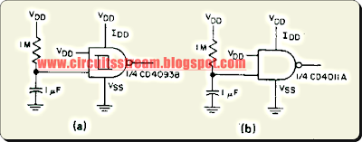
This is a simple power on switching circuit. This type of reset pulse is ideally provided by this circuit. Because of the high input impedance of the Schmidt trigger, long reset pulse times may be achieved without the excess dissipation that results when both output devices are on simultaneously, as in an ordinary gate device (B). A reset pulse is often required at power-on in a digital system. See circuit diagram below.

Simple Power On Reset Circuit Diagram

Simple Power On Reset Circuit Diagram

  • Digg
  • Del.icio.us
  • StumbleUpon
  • Reddit
  • RSS

Build 32 Watt Amplifier Circuit Using by TDA2050V

Build 32 Watt Amplifier Circuit Using by TDA2050V. A 32 Watt per channel stereo power amplifier made using the TDA2050V monolithic integrated circuit.

 32 Watt Amplifier Circuit Diagram


32 Watt Amplifier Circuit Using by TDA2050V


Notes:

This circuit is for a 32 Watt stereo audio power amplifier using the TDA20501. With a dual 22 Volt supply this amplifier can deliver 32W into 8 ohm loudspeakers. Moreover, the TDA 2050 delivers typically 50W music power into 4 ohm load over 1 sec at VS= 22.5V and f = 1KHz. The amplifier is cased as a Pentawatt package see pinout below:


TDA2050V

This is a power amplifier and requires 200mV RMS for full output. Voltage gain is 30.5dB with resistor values shown. Closed loop gain is set by Ratio R1/R2. Increase R2 for less gain and vice versa. Power bandwidth is 20Hz to 80KHz. R3, C3 and R6, C11 form a zobel network to prevent high frequency instability.

The speaker is direct coupled, therefore no expensive large value electrolytics are needed and the bass will be crisp and clean. It is advisable to place fuses in the power supply (not shown).

Parts List:

R1,R4,R5,R8______22k 1/4W Resistor
R2,R7__________680R 1/4W Resistor
R3,R6___________2.2R 1/4W Resistor
C1,C10___________1u NP 25V Capacitor
C2,C12__________22u 63V Electrolytic
C3,C11_________0.47u 400V Polyester
C4,C7,C8,C9_____100n 400V Polyester
C5,C6,C13,C14___220u 63V Electrolytic
U1,U2__________TDA2050V 32W Audio Power Amp

  • Digg
  • Del.icio.us
  • StumbleUpon
  • Reddit
  • RSS

Build a Simple Digital Electronic Lock Circuit Diagram

Build a Simple Digital Electronic Lock Circuit Diagram. This is a Build a Simple Digital Electronic Lock Circuit Diagram. The digital lock shown below uses 4 common logic ICs to allow controlling a relay by entering a 4 digit number on a keypad. The first 4 outputs from the CD4017 decade counter (pins 3,2,4,7) are gated together with 4 digits from a keypad so that as the keys are depressed in the correct order, the counter will advance.

Simple Digital Electronic Lock Circuit Diagram

Simple Digital Electronic Lock Circuit Diagram


As each correct key is pressed, a low level appears at the output of the dual NAND gate producing a high level at the output of the 8 input NAND at pin 13. The momentary high level from pin 13 activates a one shot circuit which applies an approximate 80 millisecond positive going pulse to the clock line (pin 14) of the decade counter which advances it one count on the rising edge.

A second monostable, one shot circuit is used to generate an approximate 40 millisecond positive going pulse which is applied to the common point of the keypad so that the appropriate NAND gate will see two logic high levels when the correct key is pressed (one from the counter and the other from the key). The inverted clock pulse (negative going) at pin 12 of the 74C14 and the positive going keypad pulse at pin 6 are gated together using two diodes as an AND gate (shown in lower right corner). The output at the junction of the diodes will be positive in the event a wrong key is pressed and will reset the counter.

When a correct key is pressed, outputs will be present from both monostable circuits (clock and keypad) causing the reset line to remain low and allowing the counter to advance. However, since the keypad pulse begins slightly before the clock, a 0.1uF capacitor is connected to the reset line to delay the reset until the inverted clock arrives. The values are not critical and various other timing schemes could be used but the clock signal should be slightly longer than the keypad pulse so that the clock signal can mask out the keypad and avoid resetting the counter in the event the clock pulse ends before the keypad pulse.

The fifth output of the counter is on pin 10, so that after four correct key entries have been made, pin 10 will move to a high level and can be used to activate a relay, illuminate an LED, ect. At this point, the lock can be reset simply by pressing any key.

The circuit can be extended with additional gates (one more CD4011) to accept up to a 8 digit code. The 4017 counting order is 3 2 4 7 10 1 5 6 9 11 so that the first 8 outputs are connected to the NAND gates and pin 9 would be used to drive the relay or light. The 4 additional NAND gate outputs would connect to the 4 remaining inputs of the CD4068 (pins 9,10,11,12). The circuit will operate from 3 to 12 volts on 4000 series CMOS but only 6 volts or less if 74HC parts are used. The circuit draws very little current (about 165 microamps) so it could be powered for several months on 4 AA batteries assuming only intermittent use of the relay.

Sourced By : Streampowers

  • Digg
  • Del.icio.us
  • StumbleUpon
  • Reddit
  • RSS

Build a 10W 225-400mhz Linear Amplifier Circuit Diagram

Build a 10w 225-400mhz Linear Amplifier Circuit Diagram. This circuit broadband amplifier covers the 225-400 MHz military communications band producing 10 watt RF output power and operating from a 28 volt supply. The amplifier can be used as a driver for higher power devices such as 2N6439 and MRF327. The circuit is designed to be driven by a 50 ohm source and operate into a nominal 50 ohm load. 

 10W 225-400mhz Linear Amplifier Circuit Diagram


 10W 225-400mhz Linear Amplifier Circuit Diagram

The input matching network consists of a section composed of C3, C4, Z2, C5 and C6. C2 is a dc blocking capacitor, and Tl is a 4:1 impedance ratio coaxial transformer. Z1 is a 50 ohm transmission line. A compensation network consisting of Rl, Cl, and LI is used to improve the input VSWR and flatten the gain response of the amplifier. 

L2 and a small ferrite bead make up the base bias choke. The output network is made up of a microstrip L-section consisting of Z3 and C7, and a high pass section consisting of C8 and L3. C8 also serves as a dc blocking capacitor. Collector decoupling is accomplished through the use of L4, L5, C9, C10, Cll, C12, and C13.

  • Digg
  • Del.icio.us
  • StumbleUpon
  • Reddit
  • RSS

Simple Low Distortion Audio Amplifier Circuit Diagram

This is the Simple Low Distortion Audio Amplifier Circuit Diagram. The circuit was designed and sold as a card by a purveyor of surplus components but, even using mostly manufacturer's rejected transistors, we managed to get about 0.02% total harmonic distortion at 30 watts with a ±25v power supply into 8 ohms.: no bad figure even in these days of MOSFET and ICs. In 1977 anything below 0.1% was considered excellent. And this figure was pretty repeatable without doing much selection. 

The problem of course is that since I haven't touched this amplifier for many a year I have absolutely no idea what modern transistor types one should use for it but they are not critical: output transistors and drivers need to be the correct type but the other transistors can be small signal types - as long as they can handle the full voltage between + and - supplies. 

Simple Low Distortion Audio Amplifier Circuit Diagram


Simple Low Distortion Audio Amplifier Circuit Diagram


Tr1 and Tr2 are a long-tailed pair (LTP to save typing). It is quite common to have a LTP in an audio amp but this is different: this is a complimentary LTP. As far as I am aware no one else had used a complimentary LTP at the time, though I have since seen it used in one other circuit. So I guess the circuit is unique to the author. One of the things that limits the performance of a conventional LTP is that the tail source loads the common emitters. In a complementary LTP this can't happen as there is no tail current source so that all the current of one transistor has to flow through the other.

Tr2's collector current flows into D1 and D2 which develop a voltage: this is used to bias Tr8 as a constant current source for Tr4's collector. The fact that Tr4 is working at a constant current defines its base-emitter voltage which must be developed across R4. This defines a current in R4 and this is the current that the LTP must operate at - so the ring of four transistors (Tr1, 2, 3, & 4) is self biasing and all transistors work at their best with minimum unwanted loads and biasing detracting from the performance. Tr4 is actually one of the most critical transistors: in the original circuit it was selected for Vce greater than 75v. Most Texas BC212s passed easily. Lower voltage transistors caused an increase in distortion level.

There is always a down side to any circuit: in the conventional LTP the base-emitter voltages tend to cancel each other out. In the complimentary LTP they add so there is a drop of about 1.2v between the two bases: this must be cancelled in the biasing chain and, since this circuit was designed for operation over a wide range of supply voltage, I had to be a little clever. Because of the constant current operation of the LTP and the constant voltage drop across D1 & D2, there is also a constant voltage across R14. This drop is used to lift up the bottom of the biasing chain (R1 and R11) so that the output sits at around half supply voltage, over a wider supply range.

D3 and D4 develop a bias voltage so that the output transistors are at the correct point, slightly conducting, to minimise crossover distortion.

The output transistors are complimentary (the original design used MJE2011 and MJE2021) and are driven by complimentary drivers: PNP driving NPN and vice versa. This arrangement is not only pleasingly symmetrical but gives better performance that the more common Darlington arrangement - the full gain of all the transistors is used and there is more internal feedback and less voltage drop.

The output current is monitored in the two resistors R7 and R22 (180 milliohms). The current limiting is unusual in that it works inside the input ring at an earlier stage than normal. This has an advantage that the current limiting transistors do not load the drive circuitry - which will introduce distortion. The slight down side is that there may be a slight tendency to oscillation when in current limit. R3 and R14 are necessary to restrict the current availability when the current limit engages. R5 and R19 are present to make the current limit vary with the voltage across the power transistors to avoid the second breakdown region of power transistors.

The points shown connecting terminals 1-2 and 6-7 are 'scratch-through tracks'. 1 and 2 are the power and signal earths: to keep distortion in a stereo system to a minimum the currents in these must never share the same path so in a stereo system four earth wires are run to the system's common earth point - a 'spider' common earth - and this means breaking the link. The link between 6 & 7 is in the feedback path and there are times when this can usefully be broken - one 'cheapskate' was to fit a tone control circuit here (see below). It works fine but is a bit of an insult to such a low-distortion design!. A third break point is in the collector of Tr2. Breaking this shuts down the amplifier completely and safely. Is a thermal switch is to be fitted, this is the place.

Overall negative feedback is in two parts: D.c. is fed back via R13: there is 100% d.c. feedback. A.c. feedback is via R12 and R17. Note the output capacitor is inside this feedback loop (speaker connects between terminal 5 and negative) which extends the low frequency response.

Another feature is the accessibility of both ends of the output coupling capacitor: being designed for a junk shop, they didn't want to use expensive capacitors! So for extra bass performance an additional capacitor can easily be connected.

The circuit can also be driven as a low input impedance: break 6-7, short pin 8 to C4's positive and apply input to pin 6. In this mode the input distortion is actually better: my original notes show as low as 0.01%!

When building a low-distortion amplifier, layout is vital. In fact to get distortion around 0.02% requires a lot of skill and experience. The problem is that the current in the output stage alternates between the two power transistors so is a 'rectified' version of the input. Now there is no such thing as a 'wire'. Any real piece of wire or copper track is a resistor with associated inductance and capacitance. If the high current, rectified output signal mixes in the same 'piece of wire' with the input signal the distortion in the rectified output current will feed into the input and cause the overall distortion to rocket. This is something which cannot properly be taught but has to be experienced. A skilled audio engineer will spend his lifetime learning about it.

Another interesting idea which is not shown is to fit a resistor between pin 3 and R18. This decreases the current at higher voltages and allows it to increase at low supply voltages. My notes show that this had a considerable advantage for low voltage operation because it increases the bias. It also is positive feedback which increase the open-loop voltage gain. It never got incorporated and I don't remember the details.

Tone controls

Tone controls

The circuit shows a simple (but effective) way of adding tone controls around the power amp. This does increase the distortion a little so it is not as 'hi-fi' a solution as a separate tone control stage, but it is simple and quite effective.

To use the tone controls you must break the link between 6 and 7 on the circuit. Also the 150K resistor, R13, should be decoupled. Replace it by two 68K resistors in series. The centre point of these two connects to the positive of a 1µ electrolytic whose negative connects to the earth (0v) line. This stops R13 acting as negative feedback which otherwise would shunt the tone controls.


Sourced by : Author: Richard Torrens
Site hosted by Arachsys

  • Digg
  • Del.icio.us
  • StumbleUpon
  • Reddit
  • RSS

Build a Wideband UHF Amplifier Circuit Diagram

This is the simple wide band UHF amplifier with high-performance fetes. The amplifier circuit is designed for 225 MHz center frequency, 1 dB bandwidth of 50 MHz, low input VSWR in a 75-ohm system, and 24 dB gain Three stages of U310 FETs are used in a straight forward design.


Wide-band UHF Amplifier Circuit Diagram


Wideband UHF Amplifier Circuit Diagram

  • Digg
  • Del.icio.us
  • StumbleUpon
  • Reddit
  • RSS

Simple Inverse Scalier Circuit Diagram

Simple Inverse Scalier Circuit Diagram. If a DAC is operated in the feedback loop of an operational amplifier, then the amplifier gain is inversely proportional to the input digital number or code to the DAC.The version giving scaling inversely proportional to positive voltage is shown.


Simple Inverse Scalier Circuit Diagram


  • Digg
  • Del.icio.us
  • StumbleUpon
  • Reddit
  • RSS

Build a Cmos line Receiver Circuit Diagram

Build a Cmos line Receiver Circuit Diagram. This is a simple  Cmos line Receiver Circuit Diagram, in this circuit the trip point is set half way between the supplies by Rl and R2; R3 provides over 200 mV of hysteresis to increase noise immunity. Maximum frequency of operation is about 300 kHz. If response to TTL levels is desired, change R2 to 39 K. The trip point is now centered at 1 V.

Cmos line Receiver Circuit Diagram


  • Digg
  • Del.icio.us
  • StumbleUpon
  • Reddit
  • RSS

Simple Remote on-off Switch Circuit Diagram

Simple Remote on-off Switch Circuit Diagram. This circuit provides power control without running line-voltage switch leads. The primary of a 6-volt filament transformer is connected between the gate and one of the main terminals of a triac. 

 Simple Remote on-off Switch Circuit Diagram


Simple Remote on-off Switch Circuit Diagram

The secondary is connected to the remote switch through ordinary low-voltage line. With switch open, transformer blocks gate current, prevents the triac from firing and applying power to the equipment. Closingthe switch short-circuits the secondary, causing the transformer to saturate and trigger the triac.

Sourced By circuitsstream

  • Digg
  • Del.icio.us
  • StumbleUpon
  • Reddit
  • RSS

Build a Fast Breaker Circuit Diagram

This is the simple and Fast Breaker Circuit Diagram. This 115 Vac, electronic circuit breaker uses the low drive power, low on resistance and fast turn off of the TMOS MTM15N50. The trip point is adjustable, LED fault indication is provided and battery power provides complete circuit isolation. The two `circuit breaker` terminals are across one leg of a full wave diode bridge consisting of D1-D4. Normally, Q1 is turned ON so that the circuit breaker looks like a very low resistance. 

 Fast Electronic Breaker Circuit Diagram


One input to comparator Ul is a fraction of the internal battery voltage and the other input is the drop across zeners D6 and D7 and the voltage drop across R1. If excessive current is drawn, the voltage drop across Rl increases beyond the comparator threshold (determined by the setting of R6), U1 output goes low, Q1 turns OFF, and the circuit breaker `opens.` When this occurs, the LED fault indicator is illuminated.

  • Digg
  • Del.icio.us
  • StumbleUpon
  • Reddit
  • RSS

Simple Touch Sensitive Switch Circuit Diagram

This is a Simple Touch Sensitive Switch Circuit Diagram. This circuit A high impedance input is provided by Ql, a general purpose field effect transistor 741 op amp is used as a sensitive voltage level switch which in turn operates the current Q2, a medium current PNP bipolar transistor, thereby energizing the relay which can be used to control equipment, alarms, etc.

Simple Touch Sensitive Switch Circuit Diagram


Simple Touch Sensitive Switch Circuit Diagram

  • Digg
  • Del.icio.us
  • StumbleUpon
  • Reddit
  • RSS

Simple PC Serial Port Receiver Circuit Diagram

Simple PC Serial Port Receiver Circuit Diagram. This circuit was designed to control a 32 channel Christmas light show from the PC serial port. Originally designed with TTL logic, it has been simplified using CMOS circuits to reduce component count. It is a fairly simple, reliable circuit that requires only 4 common CMOS chips (for 8 outputs), an optical isolator, and a few discrete components. The schematic diagram (SERIAL.GIF) illustrates the circuit with 16 outputs which can be expanded with additional 8 bit shift registers.

 Simple PC Serial Port Receiver Circuit Diagram

Simple PC Serial Port Receiver Circuit Diagram


Disclaimer
This circuit requires physical connections be made to the computer's serial port (COM1 or 2). To the best of my knowledge, it is difficult to cause damage to yourself or your computer by improper connections to this port, but there is no guarantee that damage will not result. Use caution when making any external electrical connections.

Basic RS232 serial transmission
Serial data is transmitted from the PC as a series of positive and negative voltages on a single wire which occur at predetermined times established by the baud rate. Both the transmitter and receiver must be operating at the same baud rate so that the receiver knows when to expect the next bit of information. For the PC serial port, baud rate and bit rate are the same thing, but this is not necessarily true with modems that can detect more than two states of the line.

In the quiescent state, with no load on the line, the voltage on the transmit line (pin 2 of the 25 pin connector) will be about -12 relative to the signal ground (pin 7), which corresponds to a logical "1". The output impedance of the serial port is about 1K ohm which yields about 6 milliamps at 6 volts. A typical data transmission frame consists of a start bit, 8 data bits, and one to three stop bits. The start bit which is always positive, signals the beginning of the transmission and is used by the receiver to synchronize the clock so that the data bits can be sampled at the proper times. After the 9th time interval passes (start bit plus 8 data bits) a dead time occurs which allows the receiver time to get ready for the next character. This dead time is referred to as a stop bit, which is always negative or the same as the quiescent state. The circuit described here requires two stop bits of dead time for reliable operation. More sophisticated circuitry would require only one.

Transmitted character examples
The letter "A" has a ASCII decimal value of 65. The "1" and "64" bits are transmitted as a negative voltage (logical "1"), and the others are transmitted as a positive voltage (logical "0"). 64 + 1 = 65 = "A"

Circuit operation
The input terminals (pins 1 and 2) of the optical isolator are connected through a 1K resistor to the transmit and signal ground pins of the PC's serial port (pins 2 and 7 of the 25 pin connector). A small signal diode is connected across the isolator input terminals to protect the isolator from reverse voltage. In the idle state, the isolator input voltage will be about -0.7 volts and the isolator LED and transistor will be off. When a start bit is received, about 5 milliamps will flow through the isolator LED causing the isolator transistor to conduct at about 80 microamps which in turn causes the external switching transistor (Q1) to turn off. The rising voltage at the collector of Q1 is coupled through a 510 pF capacitor to produce a narrow positive pulse which sets the Q output of the first RS data latch (1/2 CD4013) and enables the dual NAND gate clock oscillator.

The clock oscillator runs at a frequency equal to the baud rate (9600 Hz) and must maintain a frequency accuracy of less than 5% over the temperature range. High stability R and C components are recommended. The clock output is delayed by one cycle so that the start bit will not be received as a valid data bit. This is accomplished by the two remaining NAND gates (1/2 CD4093) and the second RS data latch (1/2 CD4013). One of these gates is used to invert the clock phase so that the first clock edge seen by the latch (clock pin 11) will be going the wrong direction and so ignored. The remaining gate, which is enabled by the second latch, opens on the third clock edge, but also inverts the clock phase, and so supplies a falling clock edge to the counter and shift registers which is again the wrong direction, and is ignored. The fourth clock edge will be rising and active and will occur near the middle (about 52 microseconds) of the first data bit which will be shifted into the registers. The remaining 7 bits are shifted into the registers on each successive rising clock edge. Data is inverted at the register outputs, a logical "1" will correspond to zero volts, and a logical "0" will correspond to +6 volts. Transmitting character (255) will set all outputs low, and transmitting character (0) will set them all high.

The 4017 decade counter increments one count on each rising clock edge and resets both data latches on the 8th edge. This in turn stops the clock and resets the counter, and the circuit remains in a waiting state until the next start bit arrives. Two stop bits of dead time are required to allow the voltage at the input of the NAND gate (pin 2) to reach a logic "1" before the next start bit arrives. Erratic operation may occur when 2 or more characters are transmitted as a string and only one stop bit is used.

The circuit may be modified to run at different baud rates by adjusting the clock frequency. This can be accomplished by temporally connecting pin 6 of the CD4013 to the positive supply and then selecting R and C values for the desired frequency. You may need to use a 1% resistor or a couple 5% resistors in series or parallel to get the value close enough. Or use a variable resistor in series of about 10% the total value.

At 9600 baud, data output at the shift registers will be unstable for about a millisecond per word while the incoming data bits are shifted into the registers and the existing bits are shifted out (into bit heaven). Higher baud rates will reduce this time proportionally and the original circuit operates at 57.6K baud to eliminate a slight flickering of the lights which was noticed at 9600.

The 74HCT164 shift register outputs will sink or source about 4 milliamps at 6 volts which can be increased with medium power transistors or FETs to drive relay coils, incandescent lights and other electronic devices. If relays are used, a small signal diode will need to be added across the relay coil to suppress the inductive voltage.

Power supply
It is recommended that 0.1 uF capacitors be installed near the power pins of each CMOS device and a well regulated/filtered power supply be used. For test purposes, a 6 volt battery will work but the clock frequency will change slightly with power supply voltage variations.

Serial port male D-SUB connectors as seen from outside the PC.

Output / Input 25 pin 9 pin
Transmit Data O 2 3
Receive Data I 3 2
Request To Send O 4 7
Clear To Send I 5 8
Data Terminal Ready O 20 4
Data Set Ready I 6 6
Ring Indicator I 22 9
Data Carrier Detect I 8 1
Signal ground - 7 5
Power line ground - 1 -

QBasic test program for 8 bit receiver
CLS
DEFINT A-Z
PRINT "Test sequence in progress, press any key to quit."
OPEN "COM1:9600,n,8,2,CD0,CS0,DS0,OP0,RS,TB2048" FOR OUTPUT AS #1
Sequence:
     FOR Bit = 0 TO 7
     PRINT #1, CHR$(255 - (2 ^ Bit));   ' Set one of 8 outputs high.
     SLEEP 1                                           ' Wait 1 sec between characters.
     IF INKEY$ <> "" THEN CLOSE : SYSTEM
     NEXT Bit


Sourced By Bill Bowden

  • Digg
  • Del.icio.us
  • StumbleUpon
  • Reddit
  • RSS

Build a 32W Amplifier Circuit Diagram Using by TDA2050V

Build a 32W Amplifier Circuit Diagram Using by TDA2050V. This is a simple circuit diagram, 32w per channel stereo power amplifier made using the TDA2050V monolithic integrated circuit.

32W Amplifier Circuit Diagram 

32W Amplifier Circuit Diagram


Notes:

This circuit is for a 32 Watt stereo audio power amplifier using the TDA20501. With a dual 22 Volt supply this amplifier can deliver 32W into 8 ohm loudspeakers. Moreover, the TDA 2050 delivers typically 50W music power into 4 ohm load over 1 sec at VS= 22.5V and f = 1KHz. The amplifier is cased as a Pentawatt package see pinout below:

TDA2050V

This is a power amplifier and requires 200mV RMS for full output. Voltage gain is 30.5dB with resistor values shown. Closed loop gain is set by Ratio R1/R2. Increase R2 for less gain and vice versa. Power bandwidth is 20Hz to 80KHz. R3, C3 and R6, C11 form a zobel network to prevent high frequency instability.

The speaker is direct coupled, therefore no expensive large value electrolytics are needed and the bass will be crisp and clean. It is advisable to place fuses in the power supply (not shown).

Parts List:

R1,R4,R5,R8______22k 1/4W Resistor
R2,R7__________680R 1/4W Resistor
R3,R6___________2.2R 1/4W Resistor
C1,C10___________1u NP 25V Capacitor
C2,C12__________22u 63V Electrolytic
C3,C11_________0.47u 400V Polyester
C4,C7,C8,C9_____100n 400V Polyester
C5,C6,C13,C14___220u 63V Electrolytic
U1,U2__________TDA2050V 32W Audio Power Amp

  • Digg
  • Del.icio.us
  • StumbleUpon
  • Reddit
  • RSS