Solar Panel Current Meter Circuit Diagram

This circuit is used to measure the current from a solar panel. It has very low power loss for currents in the 0-10A range. It also works as a general purpose DC current meter. The circuit can be used on either the positive or negative side of a DC circuit.

Solar Panel Current Meter Circuit Diagram

Solar Panel Current Meter Circuit Diagram


Specifications


Measured Current: 0-10 Amps DC, can be increased by changing the resistors.
Circuit Voltage: Will work with DC circuits at any practical voltage.
Accuracy: approximately 2% with a high quality meter movement.

Theory

The current to be measured flows through the 0.01 ohm resistor, this causes a small voltage drop across the resistor. 10 amps of current will produce a 100mV voltage across the resistor. The 100 microamp meter is wired in series with a 50 ohm fixed resistor and a 500 ohm variable calibration resistor so that it can measure the voltage drop.

The 500 ohm variable resistor is used to adjust the meter's full scale reading. The 50 ohm resistor limits the maximum current through the meter. The series resistance of the meter, the 500 ohm (or less) variable resistor and 50 ohm resistor should total 1000 ohms. Different meters may require a different variable resistor to achieve the 1000 ohm value.

Construction

Build the meter into a metal box with the meter and two connectors mounted on the outside of the box. Be sure to use connectors and wiring that are large enough to handle the full amperage from your PV array.

Alignment

Put the meter circuit in series with a known current meter such as a digital VOM meter set to measure current. Run a known current through both meters. Adjust the 500 ohm resistor until both meters read the same current. A good way to get a known current is to put a 12V lead acid battery in series with a 2 ohm 100 watt current limiting resistor. This will produce approximately 6 Amps of current. Put the two meters in series with this loop and adjust for the same reading. Beware, the resistor will get fairly hot in a short time.

A PV panel is naturally current-limited and would also work well for alignment of this meter. Just wire the panel and two meters in a series loop and adjust the calibration potentiometer for the same reading.

Use

Connect this circuit in series with a nominal 12V or 24V solar panel array. The meter can go in either the positive or negative side of the solar panel circuit. Negative side wiring can be safer from short circuit hazards. The current flowing through the solar panel to the load will be shown on the meter.

Note that the wiring in a PV system is slightly resistive and will have a measurable voltage drop. You can take advantage of that by using the system's wiring in place of the 0.01 ohm resistor. Just connect a small signal-wire to two places on either the positive or negative side of your PV system's feed wiring and send that to the meter and its two series resistors. Typical connection points would be at the PV panel's negative terminal on one side and where the PV's negative line connects to the charge controller on the other side.

The voltage drop across the PV wiring will vary with the wire gauge, the wire length and the maximum PV current. It may be necessary to adjust the value of the two series resistances and possibly the meter rating depending on the current to be measured.

Parts

1x 100 microamp DC meter
1x 0.01 ohm 5 W resistor
1x 50 ohm 1/4 W resistor
1x 500 ohm 10 turn variable resistor
2x banana plugs or a 2 pin screw type terminal block.
1x metal box

  • Digg
  • Del.icio.us
  • StumbleUpon
  • Reddit
  • RSS

Build a 16 LED Chaser Circuit Diagram

This 16 LED Chaser Circuit Diagram is a double direction flash. Similar to Digital Ping- Pong 1, there is a movement of a lit dot, up and down along the LED's length.

16 LED Chaser Circuit Diagram

16 LED Chaser Circuit Diagram


When the D16 lit the situation changes and there is a reverse movement. Lit D15-14 ……D16, is lit making circles when the circuit is under power. The IC1 is an unstable flip- flop supplying with stable frequency pulses (the frequency can be changed by TR1, adjusting the velocity of the LED's up and down).

This frequency supplies the IC3 (which is a 4-Bit UP and DOWN counter) through 2 gates A-B of the IC2. The output counter supplies the IC4 that is the driver of the LED's. The parts C- D of The IC2, make a R-S flip- flop, that changes situation, when the edge LED's D1 and D16 lit.

We have an electronic limit for the situation change. In proportion the shape we make with the LED's, we can have the proportionate optional result, making various effects.

Part List

R1= 100Kohms
R2= 220Kohms
R3= 470 ohms
TR1= 1Mohms
C1= 330nF 100V MKT
D1-16= LED 5mm
IC1= 555
IC2= 7400
IC3= 74193
IC4= 74154

  • Digg
  • Del.icio.us
  • StumbleUpon
  • Reddit
  • RSS

Simple Power Pulse Using by LM350 and NE555 Circuit Diagram

This Power Pulse Using by LM350 and NE555 Circuit Diagram can use to drive lamp,power LED,DC motor etc. Adjust R5 for output amplitude.Adjust R1 for output power .The LM350 is adjustable 3-terminal positive voltage regulators is capable of supplying in excess of 3A over a 1.2V to 33V output range.This circuit requires 5-15V power supply.


Power Pulse Using by LM350 and NE555 Circuit Diagram

Power Pulse Using by LM350 and NE555 Circuit Diagram


  • Digg
  • Del.icio.us
  • StumbleUpon
  • Reddit
  • RSS

4A High-Speed Low-Side Gate Driver Circuit

 The UCC27518 and UCC27519 single-channel, high-speed, low-side gate driver device is capable of effectively driving MOSFET and IGBT power switches. Using a design that inherently minimizes shoot-through current, UCC27518 and UCC27519 are capable of sourcing and sinking high, peak-current pulses into capacitive loads offering rail-to-rail drive capability and extremely small propagation delay typically 17 ns.

  4A High-Speed Low-Side Gate Driver Circuit

 4A High-Speed Low-Side Gate Driver Circuit


 The UCC27518 and UCC27519 provide 4-A source, 4-A sink (symmetrical drive) peak-drive current capability at VDD = 12 V. The UCC27518 and UCC27519 are designed to operate over a wide VDD range of 4.5 V to 18 V and wide temperature range of -40°C to 140°C. Internal Under Voltage Lockout (UVLO) circuitry on VDD pin holds output low outside VDD operating range.


Features
  • Low-Cost, Gate-Driver Device Offering Superior Replacement of NPN and PNP Discrete Solutions
  • Pin-to-Pin Compatible With TI’s TPS2828 and the TPS2829
  • 4-A Peak Source and 4-A Peak Sink Symmetrical Drive
  • Fast Propagation Delays (17-ns typical)
  • Fast Rise and Fall Times (8-ns and 7-ns typical)
  • 4.5-V to 18-V Single Supply Range
  • Outputs Held Low During VDD UVLO (ensures glitch free operation at power-up and power-down)
  • CMOS Input Logic Threshold (function of supply voltage with hysteresis)
  • Hysteretic Logic Thresholds for High Noise Immunity
  • EN Pin for Enable Function (allowed to be no connect)
  • Output Held Low when Input Pins are Floating
  • Input Pin Absolute Maximum Voltage Levels Not Restricted by VDD Pin Bias Supply Voltage
  • Operating Temperature Range of -40°C to 140°C
  • 5-Pin DBV Package (SOT-23)
Device Uses
  • Switch-Mode Power Supplies
  • DC-to-DC Converters
  • Companion Gate Driver Devices for Digital Power Controllers
  • Solar Power, Motor Control, UPS
  • Gate Driver for Emerging Wide Band-Gap Power Devices (such as GaN)

  • Digg
  • Del.icio.us
  • StumbleUpon
  • Reddit
  • RSS

Touch Controlled Mute Switch Circuit Diagram

Here is another simple circuit to mute the volume of Audio devices through simple touch. It exploits the action of the flip-flops in the timer IC 555 to reduce the volume of the Audio amplifier. IC NE555 is designed in the toggle mode. Its lower and upper comparator inputs are connected to the touch plates which can be membrane switches or two pieces of conducting plates. The inputs of comparators are stabilized through R1 and R2 to avoid floating.

Touch controlled Mute switch circuit diagram

 Touch Controlled Mute Switch Circuit Diagram

 
When the touch plate connected to pin 2 is touched momentarily, output of IC1 goes high and T1 conducts. The centre tap of the volume control is connected to the collector of T1. So when T1 conducts current going to the amplifier drains through T1. This reduces the volume.IC1 remains latched in this position with LED on. When the touch plate connected to pin 6 is touched momentarily, output of IC1 goes low and T1 turns off. This restores the volume.

  • Digg
  • Del.icio.us
  • StumbleUpon
  • Reddit
  • RSS

SMD FM Transmitter Circuit

Let’s construct a low-power FM transmitter using surface-mount devices (SMD) that will be received with a standard FM radio. Soldering surface mounted devices is not so hard and actually is quite easy. There are many designs for small FM transmitters but they have some problems. First, you need an audio amplifier to get enough modulation. Second, the antenna is attached directly to the collector.

Third, the coil L must be wound by hand and adjusted by stretching. It all ads with a weak signal that tends to drift in frequency. In contrastm the transmitter schematic we present here eliminates some of those problems, using varactor diode for tuning and modulation, givind great sensitivity without an audio amplifier. 

FM Transmitter – How it works
The figure below shows the schematic of the transmitter which consists of two stages: an oscillator and an output amplifier. Modulation is from an electret microphone but you can use a low power audio source. 

Oscillator stage
Transistor Q1 is a Colpitts oscillator where the frequency is determined by the parallel resonant circuit formed by inductor L, varactor V1 and capacitors C7 and C8. Q1 is a common-collector amplifier where the power gain counts. V1 is actually a dual varactor that eliminate the possibility of forward conduction at the sinewave peaks.

The frequency of oscillation is set by adjusting the DC voltage on V1 with potentiometer R2. R4 and C3 form a low-pass filter to prevent RF from feeding back onto the DC. 

Capacitors C7 and C8 form an AC voltage divider to provide feedback at the emitter of Q1 to sustain oscillation. A necessary condition for oscillation to start is for the radio (C7+C8)/C7 to be sufficiently bigger than 1.

SMD transmitter circuit Diagram
  
Frequency Modulation
Modulation is done by superimposing an audio signal from the electret mic onto the DC bias applied to V1. R3 and C1 form a low-pass filter to prevent RF from feeding back to the mic. R3, R4 and R2 form a votage divider for the audio. 

Transmitter output stage
The output of the oscillator is fed through C9 to the Q2 emitter-follower. The output of Q2 drives the antenna through C11. The Q2 emitter-follower it ensures that the oscillator is not loaded down by the impedance of the antenna and it provides power gain to drive the antenna.

SMD Transmitter layout
The figure below shows the layout of the PCB and it uses surface-mounted devices like resistors and capacitors (non-polar devices). All the caps are size 0805 and all resistors are size 1206. use through-hole components for Q1, Q2, IC1 and V1. You can use an SOT-89 device for IC1 and an SOT-23 device for V1. Use MPSH10 or a transistor equivalent. Here you can learn how to solder smd chips 

SMD transmitter circuit Diagram

  
The inductor
A coil would consist of two or three turns of wire but for this schematic we will use an inductor with loops of copper on the PCB. Such flat spiral inductor are common at these frequencies.
One formula for flat spiral inductors is:
flat spiral inductors formula where
L = inductance in uH
r = radius of coil (outer radius + inner radius divided by 2 ) inches
N = number of turns
d = depth of coil (outer radius minus inner radius) inches 

Tuning range
While commercial FM band goes from about 88 MHz to 108 MHz, the L and C values used in this design allow tuning up to 100 MHz.

Transmitter testing
You will need a portable FM radio and an assistant. First, find an empty spot on the FM dial and set your radio about 30 feet away (9 meters). The radio’s volume control should not be set too high to prevend feedback. Next, power-up your transmitter and talk to yourself as you adjust the frequency with the trim-pot. When your assintant hears you, your transmitter is tuned. You might have to adjust the radio’s tuner slightly for best reception.

Have fun with it but remember that using the transmitter as a bugging device may not be legal in your country. To use the circuit as a wireless microphone, increase the value of R3. The transmitter range is about 100 feet (30 meters) inside a building. 

Parts list

SMD transmitter circuit Diagram
 

  • Digg
  • Del.icio.us
  • StumbleUpon
  • Reddit
  • RSS

Build a Cell Phone Jammer Schematic Diagram

Build a Cell Phone Jammer Schematic Diagram
 
This cell phone jammer operates at GSM800 frequency since most mobile phones use it to operate. So the selected VCO is a sweeping oscillator, which is very effective but may be hard to construct for the beginners without nice RF-testing equipment.

As a noise source you can use 45MHz clock oscillator which is driving Local Oscillator port located on a mini-circuit mixer. There is also an impedance matching network for Local Oscillator signal to pass through it. It is used to equate impedances of the clock oscillator and the port of the mixer.

RF input (which is this port of the mixer) connected to the first 800MHz cell phone antenna, and the RF output is sent to the mini-circuit amplifier. This amplifier increases the output power for 15-16dbm. The amplified signal then sent to the second cell phone antenna.

Build a Cell Phone Jammer Schematic Diagram


 works
All cell phones which use GSM800 have their transmitted and received frequencies always separated by 45MHz. So when the mobile phone tries to call it is blocked by its own signal returning to it! Isn’t that cool? When the phone blabber annoys you – turn your jammer on and that wrongdoer will hear own voice in his or her cell phone.

Oh, by the way, you can also use this mobile signal jammer to block any cell-based tracking systems which use your GPS to track and record your car’s moves. And it is quite possible (though I didn’t actually tested it) to jam IEDs which detonated using cell phones.

Build a Cell Phone Jammer Schematic Diagram


The mixer used is designed to work up to 600MHz but in this case it works pretty well.

Build a Cell Phone Jammer Schematic Diagram
 
RF amplifier is doing its job perfectly yet (as it was mentioned in the Jammer Store blog post) draws additional power.Old aluminium box was used as a frame for the jammer and old UHF connectors from Motorola cell phone as input/output.You need to attach RF connectors to the circuit. Nine volt battery and voltage regulator were used to supply all components. The battery was placed inside and separated by the foamed plastic from the other components.The power on/off switch is placed on the top. The input and output antennas (also from old Motorola mobile phone) are screwed onto UHF connectors.Your cell phone jammer is ready. Enjoy!

Build a Cell Phone Jammer Schematic Diagram


  • Digg
  • Del.icio.us
  • StumbleUpon
  • Reddit
  • RSS

Amid weak sales, Nintendo will drop Wii U price by $50

Amid weak sales, Nintendo will drop Wii U price by $50

In a press release today, Nintendo announced that starting Sept. 20, the Wii U Deluxe set would sell for $299.99, down from $349.99 at launch. Also on Sept. 20, Nintendo will release a Legend of Zelda: Wind Waker bundle – complete with the game, a bunch of limited-edition artwork, and a "GamePad with Zelda-inspired gold accents" – for $299.99. 

So what's behind the announcement? Well, for one thing, the Wii U has been selling rather dismally. According to Reuters, Nintendo has unloaded 3.6 million Wii U units since launch, which sounds like a big number until you consider that the Wii U launched all the way back in November of 2012. Globally, in the months spanning April 1 and June 30, the Wii U sold a measly 160,000 units. (That figure is "really, really bad" Kotaku has noted.) 

But there's also the small matter of the impending launch of the Microsoft Xbox One and Sony PlayStation 4. Microsoft is said to be eyeing a Nov. 8 release date for its device; Sony has confirmed that the PS4 will hit shelves on Nov. 15 in the US and Canada. (To put things in perspective, the PS4 will sell for $399 and the Xbox One for $499, but then again, both consoles are considerably more powerful than the Wii U.) 

The press maelstrom that is likely to follow the debut of both devices certainly won't be good for Nintendo, which puts extra pressure on the Japanese company to get consumers interested in the ailing Wii U.
And who knows? If there's one thing that can rouse a torpid fan base, it's a new Zelda game. [via]

  • Digg
  • Del.icio.us
  • StumbleUpon
  • Reddit
  • RSS

Build a18W Car Stereo Amplifier Circuit Diagram

This automobile stereo amplifier project is a class AB audio power amplifier using the Hitachi HA13118 module. It not only can be used in automobile application but also in any transportable or home amplifier process. It is simple to construct & has a maximum of outside parts. The module has a high power output from a low voltage supply using the bridge tied load system, & a high gain of 55dB.

This project will be useful in applications where the input signal is a low level, without requiring the use of a separate pre-amplifier. This IC module has a built in surge protection circuit, thermal shutdown circuit, ground fault protection circuit & power supply fault protection circuit making it reliable.
The Specifications of this project 
D.C. Input : 8 – 18V at 1-2 A

Power output : 18W maximum, 4 ohm load, 18V DC supply

S/N ratio : > 70 dB

THD : < 0.2% @ 1W

Freq. Response : ~ 30 Hz to 30 kHz, –3 dB

Input level : < 25 mV, for full output (G > 50dB)

Input Impedance : ~ 30 k ohm

The supply voltage necessary for this project is 8 -18V DC, at least one to two Amps. Maximum output power will only be obtained with a power supply of 18V at greater than two A, using a four ohm speaker. The power supply ought to be well filtered to reduce mains hum, a regulated supply will reduce noise even further. Additional filtering is unnecessary if operating from a battery supply.

Circuit Diagram Description

Most of the circuitry is contained within the amplifier module. C10 is the input coupling capacitor and blocks DC from the input. C11 bypasses any RF which may be present at the input. C1 & C2 provide an AC ground for the inverting inputs of the IC. R1/C7 and R2/C8 provide a high frequency load for stability with difficult speakers. C five & C six provide bootstrap feedback for the IC. C9 & C12 provide power supply filtering.

Build a18W Car Stereo Amplifier Circuit Diagram

An externally mounted logarithmic potentiometer of between 10k ohm and 50k ohm, is used depending on the desired input impedance. The impedance ought to be keep as high as feasible for a guitar amp, unless using a separate pre-amp. Make sure-that the heat sink is mounted to the module.


  • Digg
  • Del.icio.us
  • StumbleUpon
  • Reddit
  • RSS

Build a Telephone Record Control Circuit Diagram

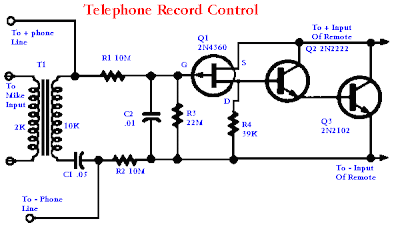
This simple Telephone Record Control Circuit Diagram will allow you to connect any tape recorder that has a mic and remote input to a phone line and automatically record both sides of a conversation when ever the phone is in use. You will need to take a couple of voltage readings before connecting the circuit. First determine the polarity of your phone line and connect it to the circuit as shown and then determine the polarity of the remote input and connect it to the circuit.

Circuit operation is as follows. When the phone is on hook the voltage across the phone line is about 48volts dc. When the phone is off hook the voltage will drop to below 10volts dc. When the line voltage is at 48volts the FET is off which causes Q2 and Q3 to be off. When the phone is picked up the FET turns on along with Q2 and Q3 which turns your recorder on. The tape recorder must be in the record mode at all times. As you can see the power source for the circuit is the phone line. 

Telephone Record Control Circuit Diagram

Telephone Record Control Circuit Diagram
 

  • Digg
  • Del.icio.us
  • StumbleUpon
  • Reddit
  • RSS

Simple Telephone In Use Indicator Circuit Diagram

This is a Simple Telephone In Use Indicator Circuit Diagram. With this circuit mounted in or near every phone in the house, it will allow users to know if the phone is being used and not to pick up the phone. When a phone is taken off hook, the voltage across the tip and ring terminals drops to 10 volts or less. This will cause the FET (2N4360) to turn on and also turn on the transistor (2N2222). When the transistor turns on it will allow current to flow through the LED and make it light. A blinking LED could be used to make the effect better. 

Simple Telephone In Use Indicator Circuit Diagram


  • Digg
  • Del.icio.us
  • StumbleUpon
  • Reddit
  • RSS

Simple FM Transmitter Circuit Diagram

This circuit is a simple two transistor (2N2222) FM transmitter. No license is required for this transmitter according to FCC regulations regarding wireless microphones. If powered by a 9 volt battery and used with an antenna no longer than 12 inches, the transmitter will be within the FCC limits.

The microphone is amplified by Q1. Q2, C5, and L1 form an oscillator that operates in the 80 to 130 MHz range. The oscillator is voltage controlled, so it is modulated by the audio signal that is applied to the base of Q2. R6 limits the input to the RF section, and it's value can be adjusted as necessary to limit the volume of the input. L1 and C6 can be made with wire and a pencil. The inductor (L1) is made by winding two pieces of 24 gauge insulated wire, laid side by side, around a pencil six times. Remove the coil you have formed and unscrew the two coils apart from each other. 

  FM Transmitter Circuit Diagram

  FM Transmitter Circuit Diagram


One of these coils (the better looking of the two) will be used in the tank circuit, and the other can be used in the next one you build. The antenna (24 gauge wire) should be soldered to the coil you made, about 2 turns up from the bottom, on the transistor side, and should be 8-12 inches long. To make C6, take a 4 inch piece of 24 gauge insulated wire, bend it over double and, beginning 1/2" from the open end, twist the wire as if you were forming a rope. When you have about 1" of twisted wire, stop and cut the looped end off, leaving about 1/2" of twisted wire (this forms the capacitor) and 1/2" of untwisted wire for leads.

  • Digg
  • Del.icio.us
  • StumbleUpon
  • Reddit
  • RSS

80mph on a bicycle!

80mph on a bicycle!


For cycling enthusiast Tom Donhou, there has only ever been one mission. To ride as fast as he possibly can on two wheels.

In a bid to prove what can be achieved through backyard engineering, he has custom-built a bike which reached speeds of up to 80mph.

A London-based bicycle frame builder by trade, Donhou invented a 104-tooth chainring to achieve the goal. And in another tribute to British engineering, he wanted to use a car to block the wind to reduce wind traction.

The current land speed record for a bike (not bycycle) is 167mph which was set by Fred Rompelberg using a dragster in the Salt Flats.[via]

  • Digg
  • Del.icio.us
  • StumbleUpon
  • Reddit
  • RSS

iPhone 6 concept shows thinner handset with touch-sensitive home button and 12MP camera

iPhone 6 concept shows thinner handset with touch-sensitive home button and 12MP camera

Created by Arthur Reis, a budding designer who aspires to join the ranks of Jony Ive and Shin Nishibori someday, 3D renderings of the iPhone 6 imagine a handset that looks largely identical to iPhone 5 (think: anodised aluminium casing with chamfered edges), but an impressive 20 per cent slimmer at just 6.1mm thick.

iPhone 6 concept shows thinner handset with touch-sensitive home button and 12MP camera


The handset also features a 12-megapixel camera with an ‘iSight Pro’ sensor boasting an f/1.8 aperture and a ‘Magic TrackPad’ that replaces the physical home button with a touch-sensitive equivalent.

As far as we’re concerned, this is one of the best iPhone concepts we’ve seen, principally because it doesn’t go crazy on novel or unrealistic features as most concepts do.

Apple is always trying to make its handsets slimmer, so a more slender iPhone is within the realms of possibility. And with Samsung upping the ante with a 13-megapixel camera on the freshly launched Galaxy S4, we can certainly expect the iPhone 6 to match its competition in the imaging stakes.

The iPhone 6 is hotly tipped to land this summer, possibly sometime in July. Although there’s still a chance that Apple might stick to an autumn release cycle for new iPhone launches.

What do you think of Reis’s iPhone 6 concept? Let us know in the comments section below.[via]

  • Digg
  • Del.icio.us
  • StumbleUpon
  • Reddit
  • RSS

Apple iCloud, iMessage Suffer Outage

SYDNEY: Tech giant Apple's iCloud and iMessage services were reportedly hit by a major outage on Thursday and Friday. 


Apple's iMessage instant-messaging platform and iCloud back-up service went offline for almost 11 hours affecting more than 3 million users. 

According to Sydney Morning Herald, the outage began at 2.30pm on Thursday and ended at 1.22am on Friday.

Apple said that users might be unable to use iCloud Documents, Photo Stream, iPhoto Journals, or Backup and Restore or send or download attachments in iMessage. 

The tech giant also reported of another issue with its iTunes store which prevented 16.6% of users from making purchases on the store for around 45 minutes on Thursday and the losses are estimated to be around 37,000 dollars a minute. 

The company did not comment on the matter, the report added.

  • Digg
  • Del.icio.us
  • StumbleUpon
  • Reddit
  • RSS

Dual Basic Motor Speed Controllers Circuit Diagram

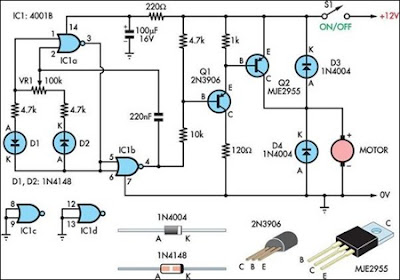
Here  are two simple 12V DC motor speed controllers that can be built for  just a few dollars. They exploit the fact that the rotational speed of a  DC motor is directly proportional to the mean value of its supply  voltage. The first circuit shows how variable voltage speed control can  be obtained via a potentiometer (VR1) and compound emitter follower (Q1  & Q2). With this arrangement, the motor’s DC voltage can be varied  from 0V to about 12V. This type of circuit gives good speed control and  self-regulation at medium to high speeds but very poor low-speed control  and slow starts. The second circuit uses a switchmode technique to vary  motor speed.

 Dual Basic Motor Speed Controllers Circuit Diagram fig 1

 Dual Basic Motor Speed Controllers Circuit Diagram fig 1

Here a quad NOR gate (IC1) acts as a 50Hz  astable multivibrator that generates a rectangular output. The  mark-space ratio of the rectangular waveform is fully variable from 20:1  to 1:20 via potentiometer VR1. The output from the multivibrator drives  the base of Q1, which in turn drives Q2 and the motor. The motor’s mean  supply voltage (integrated over a 50Hz period) is thus fully variable  with VR1 but is applied in the form of high-energy "pulses" with peak  values of about 12V.

 Dual Basic Motor Speed Controllers Circuit Diagram fig 2

 Dual Basic Motor Speed Controllers Circuit Diagram fig 2
 

This type of circuit gives excellent  full-range speed control and gives high motor torque, even at very low  speeds. Its degree of speed self-regulation is proportional to the mean  value of the applied voltage. Note that for most applications, the power  transistor (Q2) in both circuits will need to be mounted on an  appropriate heatsink.


Sourced by : Streampowers

  • Digg
  • Del.icio.us
  • StumbleUpon
  • Reddit
  • RSS

Simple Hard Disk Selector Circuit Diagram

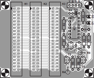
Hard Disk Selector Circuit Diagram
 
In the last few years, the available range of operating systems for PCs  has increased dramatically. Various free (!) operating systems have been  added to the list, such as BeOS, OpenBSD and Linux. These systems are  also available in different colours and flavours (versions and  distributions). Windows is also no longer simply Windows, because there  are now several different versions (Windows 95, 98, ME, NT, XP, Vista  and 7). Computer users thus have a large variety of options with regard  to the operating system to be used. One problem is that not all hardware  works equally well under the various operating systems, and with regard  to software, compatibility is far from being universal. In other words,  it’s difficult to make a good choice.

Hard Disk Selector Circuit Diagram

Hard Disk Selector Circuit Diagram


Switching from one operating system to another - that’s a risky business, isn’t it? Although this may be a bit of an exaggeration, the safest approach is still to install two different operating systems on the same PC, so you can always easily use the ‘old’ operating system if the new one fails to meet your needs (or suit your taste). A software solution is often used for such a ‘dual system’. A program called a ‘boot manager’ can be used to allow the user to choose, during the start-up process, which hard disk will be used for starting up the computer. Unfortunately, this does not always work flawlessly, and in most cases this boot manager is replaced by the standard boot loader of the operating system when a new operating system is installed.

In many cases, the only remedy is to reinstall the software. The solution presented here does not suffer from this problem. It is a hardware solution that causes the primary and secondary hard disk drives to ‘swap places’ when the computer is started up, if so desired. From the perspective of the computer (and the software running on the computer), it appears as though these two hard disks have actually changed places. This trick is made possible by a feature of the IDE specification called ‘CableSelect’. Every IDE hard disk can be configured to use either Master/Slave or CableSelect. In the latter case, a signal on the IDE cable tells the hard disk whether it is to act as the master or slave device. For this reason, in every IDE cable one lead is interrupted between the connectors for the two disk drives, or the relevant pin is omitted from the connector.

pcb

pcb

This  causes a low level to be present on the CS pin of one of the drives and  a high level to be present on the CS pin of the other one (at the far  end of the cable). The circuit shown here is connected to the IDE bus of  the motherboard via connector K1. Most of the signals are fed directly  from K1 to the other connectors (K2 and K3). An IDE hard disk is  connected to K2, and a second one is connected to K3. When the computer  is switched on or reset, a pulse will appear on the RESET line of the  IDE interface. This pulse clocks flip-flop IC1a, and depending on the  state of switch S1, the Q output will go either high or low. The state  on the Q output is naturally always the opposite of that on the Q  output. If we assume that the switch is closed during start-up, a low  level will be present on D input of IC1a, so the Q output will be low  following the reset pulse.


  • Digg
  • Del.icio.us
  • StumbleUpon
  • Reddit
  • RSS

Nokia Sells 19,000 Lumia Smartphones To Delta

Nokia Sells 19,000 Lumia Smartphones To Delta

Delta Airlines announced Thursday that it has adopted Microsoft's Windows Phone 8 platform and the Nokia Lumia 820 as its go-to handheld device for 19,000 flight attendants. The smartphones will be used to handle a range of tasks both on the ground and in the air.

 The phones are running customized software for Delta from Avanade that runs on the Microsoft Dynamics for Retail mobile point-of sale platform. Delta believes that the system, together with Wi-Fi/4G connectivity provided by AT&T, will empower its flight attendants while also improving its customers' experiences throughout the boarding, flying and deplaning processes.

The Lumia 820 is fairly compact, which makes it easy to carry around and use. It has a 4.3-inch ClearBlack display, a dual-core 1.5-GHz Snapdragon S4 processor, 1 GB of RAM, an 8-megapixel camera with Carl Zeiss optics, NFC and Nokia's suite of software.

 Together with the Avanade software, the Lumia 820 should be a powerful ally for flight attendants. It can handle near real-time credit card processing for onboard purchases, including upgrades to Delta's Economy Comfort seating, as well as food and beverage purchases. Customers can choose to have e-receipts emailed to them rather than accept a paper receipt on the plane. The system promises to speed up transactions by about 10% across the board. It is compatible with regular and prepaid credit cards, and will soon be able to read digital coupons that are displayed on a customer's mobile phone. Delta said that its flight attendants will be able to pull up flight connection details for passengers, too.[via]

  • Digg
  • Del.icio.us
  • StumbleUpon
  • Reddit
  • RSS

Purported press image of iPhone 5C appears online

While the purported iPhone 5C, Apple's low-cost iPhone, has made several online appearances, including in some really high resolution pictures and videos that surfaced on the Internet, a website now claims to have published the official press shots of the phone.  Romania based publication, Mobilissimo.ro, claims that a Romanian retailer sent a couple of press shots of the iPhone 5C to the website.  The press photo features the White coloured variant of the iPhone 5C running iOS 7.The front panel is also in White unlike some previous leaks, while the back of the phone features the same plastic polycarbonate body panel that appeared in recent leaks, in glossy White, complete with a round camera lens and LED flash, Apple logo and iPhone branding.  The left-hand side of the phone features the same pill shaped volume rocker and mute keys that had appeared online, in a recent leak. These are also White in colour.  In addition to the press pictures, the site has also posted images of what the Romania-based dealer claims as iPhone 5C dummies placed in shop shelves till the actual phone arrives. The dummy features a White plastic power button. At the bottom of the dummy phone, there's a small hole for the second microphone, next to the 3.5mm headset jack port, two screw holes with the Lightning connector port at the centre, and four holes for the speaker towards bottom right. This is in line with the pictures that appeared recently on Sonny Dickson's website.  It's interesting to note that the low-cost iPhone has leaked several times but the pictures were of pre-production units and did not feature cut outs for the power and volume rocker keys.  Other alleged pictures of the iPhone 5C have revealed a plastic polycarbonate body back panel in White, Blue, Red, Yellow and Green colours. However, we've not heard much about the specifications of the phone till now.  Apple is expected to unveil the iPhone 5C along with the iPhone 5S, the next generation iPhone, on September 10 at an event in San Francisco. It's worth pointing out that Apple has not sent any invitations or announced an event officia

While the purported iPhone 5C, Apple's low-cost iPhone, has made several online appearances, including in some really high resolution pictures and videos that surfaced on the Internet, a website now claims to have published the official press shots of the phone.

Romania based publication, Mobilissimo.ro, claims that a Romanian retailer sent a couple of press shots of the iPhone 5C to the website.

The press photo features the White coloured variant of the iPhone 5C running iOS 7.The front panel is also in White unlike some previous leaks, while the back of the phone features the same plastic polycarbonate body panel that appeared in recent leaks, in glossy White, complete with a round camera lens and LED flash, Apple logo and iPhone branding.

The left-hand side of the phone features the same pill shaped volume rocker and mute keys that had appeared online, in a recent leak. These are also White in colour.

In addition to the press pictures, the site has also posted images of what the Romania-based dealer claims as iPhone 5C dummies placed in shop shelves till the actual phone arrives. The dummy features a White plastic power button. At the bottom of the dummy phone, there's a small hole for the second microphone, next to the 3.5mm headset jack port, two screw holes with the Lightning connector port at the centre, and four holes for the speaker towards bottom right. This is in line with the pictures that appeared recently on Sonny Dickson's website.

It's interesting to note that the low-cost iPhone has leaked several times but the pictures were of pre-production units and did not feature cut outs for the power and volume rocker keys.

Other alleged pictures of the iPhone 5C have revealed a plastic polycarbonate body back panel in White, Blue, Red, Yellow and Green colours. However, we've not heard much about the specifications of the phone till now.

Apple is expected to unveil the iPhone 5C along with the iPhone 5S, the next generation iPhone, on September 10 at an event in San Francisco. It's worth pointing out that Apple has not sent any invitations or announced an event officia. [via]

  • Digg
  • Del.icio.us
  • StumbleUpon
  • Reddit
  • RSS

Over voltage Protection Circuit Diagram

When testing a circuit, a source of voltage that is variable and has over voltage shutdown is veiy useful. In this circuit, Rl is adjusted to 1 to 2 V below the eventual shutdown threshold. R2 sets the trip voltage. When this voltage is reached, the circuit shuts the voltage to the circuit under test down. To reset, reduce Rl below trip threshold and depress reset switch SI.

Over voltage Protection Circuit Diagram

Overvoltage Protection Circuit Diagram

  • Digg
  • Del.icio.us
  • StumbleUpon
  • Reddit
  • RSS

Burglar Alarm With Timed Shutoff Circuit Diagram

This is a Burglar Alarm With Timed Shutoff Circuit Diagram. When SI (sensor) is closed, power is applied to U2, a dual timer. After a time determined by C2, CI is energized after a predetermined time determined by the value of C5, pin 9 of U2 becomes low, switching off the transistor in the optoisolater, cutting anode current of SCR1 and DE-energizing Kl. The system is now reset. Notice that (i6x C2) is less than (R7xC$). The ON time is approximately given by:(R7xC5)-(R6xC2) = Ton

Burglar Alarm With Timed Shutoff Circuit Diagram

Burglar Alarm With Timed Shutoff Circuit Diagram

  • Digg
  • Del.icio.us
  • StumbleUpon
  • Reddit
  • RSS

Rare Ferrari auctioned for $27 million and it's all going to charity


Rare Ferrari auctioned for $27 million and it's all going to charity

The family of Eddie Smith has auctioned off their late father's 1967 Ferrari 275 GTB/4*S N.A.R.T Spider, and generously donated all the proceeds to charity. The rare car (only 10 were ever made) was sold Saturday night at RM Auctions in Monterey, Calif., for $27.5 million. That price set a new world record for the most expensive road car of any kind sold at auction. 

Smith took ownership of the Ferrari in 1968, and his son, Eddie Smith Jr., told the auction crowd that selling it was "a bittersweet moment." According to the Los Angeles Times, he advised its new owner to "Drive it, love it, enjoy it, and more importantly share it with others so they can see it." [Source] [Source 
]
Trending topic: ferrari auctioned | Click to see more on msnNOW.com

  • Digg
  • Del.icio.us
  • StumbleUpon
  • Reddit
  • RSS

Samsung Galaxy S3- 10 Things You Didn’t Know It Did


Samsung Galaxy S3-10 Things You Didn’t Know It Did

One of the most feature packed devices on the market at the moment is no doubt the Samsung Galaxy S3. However thanks to the fact that it comes with so many features, it can be possible to miss some. So here we show you 10 the features that you might not know existed on your Samsung Galaxy S3.

Samsung Galaxy S3 hidden features roundup (Part 4)

If you chose the Samsung Galaxy S3 due to its large display and you are not technically minded then you might be happy to know you can choose to activate an easy UI mode on your device. This means that you will have large pre-set widgets and a simplified setup. All you have to do to get the mode is go into settings and choose the home screen mode.

When you are in contacts you can easily call or text people by swiping. All you have to do is swipe left to right if you want to call someone or right to left if you want to text someone.

If you want to save battery you can use the power saving feature. This mode will change many aspects on your phone, including screen brightness, haptic feedback, CPU speed and the colour of the web browser’s background.

Those people who take videos on their Samsung Galaxy S3 will be pleased to know that editing is possible and simple. You can trim your videos on the handset via the app in the drawer.

While there isn’t video output on the handset you can get an HDMI adapter which allows you to send HD videos directly to your HD TV. You can get your hands on the adapter for around $20.

If you want to view webpages offline than you can store web pages into the memory of the Samsung Galaxy S3 and read them at any time. All you have to do is hit the soft key menu button and then pick save for offline reading.

While you can use the Kies software for transferring photos, video and other files to your handset there is also the option to drag and drop. You can also sync your Samsung Galaxy S3 through Wi-Fi thanks to it.

You are not limited to one specific video format on the device as the S3 recognises many different formats. This means that you don’t have to worry about converting video before watching it on your handset.

The Samsung Galaxy S3 comes with support for panoramic photos. This means that you can capture not just what’s in front of you, but also what’s to the sides.

If you lose your Samsung Galaxy S3 or it is stolen you have the option to wipe it remotely. You can do this by signing up to Samsung online and if your device is lost you can use the Find my Phone feature.

Finally there is a hidden Easter egg on the S3. If you want to see a Jelly Bean face on your device just keep clicking on the Android version and it will pop up. If you keep your finger pressed down on the face, your display will fill with jellybeans.[via]

  • Digg
  • Del.icio.us
  • StumbleUpon
  • Reddit
  • RSS

Apple's highly anticipated iPhone5S

Apple's highly anticipated iPhone5S
 
Apple’s iPhone5S and its cheaper version in plastic 5C are expected to be unveiled on September 10 but it might not see great levels of excitement and big crowds.

MSN Money said that the reason was a cold response can be attributed to the fact that the new iPhone is no longer a ‘cultural phenomenon’ as rivals like Samsung are making smartphones that are just as good, News.com.au reports.

iPhone 5S is expected to be of the same size as iPhone 5, which means it will still be smaller than the Samsung Galaxy S3 and S4.

MSN said that the new device may have a fingerprint reader and have ‘tweaks’ rather than real advancements and the biggest thing it will lack is major innovation, something for which the software giant was well known for during the Steve Jobs days, the report added.[via]

  • Digg
  • Del.icio.us
  • StumbleUpon
  • Reddit
  • RSS

Switch ON-OFF Touch or with Push Button Circuit Diagram

Here we have three choices, with which we can make electronic switches that use our touch or pressing (push button). We thus exploit the very big resistance of entry, that present the gates CMOS. In the fig.1 we have two gates NAND or NOR (IC1), connected as R-S flip-flop. Just as we press the switch S1, the exit 3 it becomes [H], even it is maintained in this situation.

To change the situation, it should we press switch S2. Now exit 3, takes price (L), reversely exit 4 becomes (H). In order to we maintain the situation that we want, we can connect at parallel with the corresponding switch, a capacitor C=100nF. This entry will always drive the corresponding exit to logic (L), immediately afterwards the benefit of supply to the circuit.

Switch ON-OFF Touch or with Push Button Schematic

Switch ON-OFF Touch or with Push Button Schematic


In the fig. 2, we have a circuit of inverter CMOS, in the entry of which is applied logic situation (H), from the resistance R, which the other end of, is in the supply. Exit 2 has situation (L).

When we press switch S2, in the entry of 3 IC2, we have situation (L), this it goes to the ground, the exit now becomes (H). This situations are maintained as long as we keep pressed switch S2 and they change immediately hardly the touch. If we want opposite logic operation then it will be supposed we connect the resistance R, in the ground and switch S2, in the supply. The same logic we will have if we replace gate IC2, with a gate NAND or NOR, as it appears in the fig. 3, the result is the himself.

Because the situation in the case of fig.1 and 3, does not remain constant and change when we pull our finger , in order to him we retain, it should we connect a J-K or D flip-flop as T, after the IC2 and IC3. Thus the flip-flop, will change situation, each time where we will touch the switch or will touch the contacts and him it will retain.

All the switches can be replaced with contacts, it is enough we replace also resistances R with the price of 10MΩ. The Resistances R when we use pressing switches can are, from 100KΩ until 1MΩ. Because when we use contacts instead of switches, the noise can turn on the gates of fig. 2 and 3, then can place a capacitor 100nF, parallel with the contacts.[via]

  • Digg
  • Del.icio.us
  • StumbleUpon
  • Reddit
  • RSS

Top Performance LA4446 Stereo Audio Amplifier Circuit

LA4446 is of similar series IC as LA4440, but it is meant for dual or stereo 5.5Watt RMS outputs. While 4440 gives 6Watt outputs at dual mode, this gives almost same but with much smaller package size. The IC package is mall but it provides same functionality and special features like LA4440. These are,
  1. Low pop noise at power ON/OFF time
  2. Good ripple rejection: 46dB(typ)
  3. Good channel separation
  4. Low residual noise (Rg=0)
  5. On chip protectors as Thermal protector, Over-voltage/Surge Protector, and pin short protector
The below circuit is the application circuit of LA4446 IC. 

Top Performance LA4446 Stereo Audio Amplifier Circuit

  • Digg
  • Del.icio.us
  • StumbleUpon
  • Reddit
  • RSS

Simple Voltage-to-Current Converter Drives White LEDs

You sometimes need to drive a white LED from one 1.5V battery. Unfortunately, the forward voltage of a white LED is 3 to 4V. So, you would need a dc/dc converter to drive the LED from one battery. Using the simple circuit in Figure 1, you can drive one white LED or two series-connected green LEDs, using only a few components. The circuit is a voltage-to-current converter, which converts the battery voltage to a current that passes through the LED.

You can adjust this current and, thus, the brightness of the LED, by varying resistor R3. If you turn on switch S1, resistor R2 feeds base current to transistor Q2. Q2 turns on, and its collector current, via R3, turns on Q1. Now, the current through inductor L1 increases. The slope of the increase is a function of the value of L1 and the battery voltage. The current through L1 increases until it reaches a maximum value, which depends on the gain of Q1. Because the value of R3 sets the base current drawn from Q1, Q1's collector current is also limited.

White LEDs Circuit Diagram

White LEDs Circuit Diagram


Once the current through L1 reaches its maximum value, the slope of the current through L1 changes. At that instant, the voltage on L1 switches to a negative polarity forced by the changed slope. This negative voltage traverses capacitor C1 and turns off Q2, which in turn turns off Q1. The negative voltage on L1 increases until it reaches the forward voltage of the LED. The peak current through inductor L1 now flows through the LED and decreases to zero. Now, Q2 switches on again, via the current through R2, and the cycle starts again.

By adjusting resistor R3, you can set the peak current through L1 and the peak current through the LED. The brightness of an LED is a linear function of the current through the LED. So, adjusting the value of R3 also adjusts the brightness of the LED.

It doesn't matter which LED you use; the forward voltage on the LED always increases until the peak current through L1 flows through the LED. Different forward voltages of the LEDs yield different on-times (duty cycles) but the same peak current through the LED. With the values shown in Figure 1, the circuit oscillates at a frequency of approximately 30 kHz and delivers a 20-mA peak current through the LED.

The duty cycle depends on the ratio of the battery voltage to the forward voltage of the LED. One advantage of this circuit is that it requires no series-limiting resistor for the LED. The peak current through the LED is a function of the value of R3 and the gain of Q1.[via]

  • Digg
  • Del.icio.us
  • StumbleUpon
  • Reddit
  • RSS

Build a Doorbell Circuit For Deaf People

This circuit provides a delayed visual indication when a door bell switch is pressed. In addition, a DPDT switch can be moved from within the house which will light a lamp in the door bell switch. The lamp can illuminate the words "Please Wait" for anyone with walking difficulties.

 Doorbell Circuit Diagram

 Doorbell Circuit Diagram


Notes:
The circuit uses standard 2 wire doorbell cable or loudspeaker wire. In parallel with the doorbell switch, S1, is a 1N4001 diode and a 12 volt 60mA bulb.

The bulb is optional, it may be useful for anyone who is slow to answer the door, all you need to do is flick a switch inside the house, and the bulb will illuminate a label saying Please Wait inside the doorbell switch or close to it.

The double pole double throw switch sends the doorbell supply to the lamp, the 22 ohm resistor is there to reduce current flow, should the doorbell switch, S1 be pressed while the lamp is on.

The resistor needs to be rated 10 watts, the 0.5 Amp fuse protects against short circuits.

When S2 is in the up position (shown as brown contacts), this will illuminate the remote doorbell lamp. When down, (blue contacts) this is the normal position and will illuminate the lamp inside the house. Switch S1 will then charge the 47u capacitor and operate the transistor which lights the lamp.

As a door bell switch is only pressed momentarily, then the charge on the capacitor decays slowly, resulting in the lamp being left on for several seconds. If a longer period is needed then the capacitor may be increased in value.

  • Digg
  • Del.icio.us
  • StumbleUpon
  • Reddit
  • RSS

Simple Photodiode Alarm Circuit Diagram

  • Digg
  • Del.icio.us
  • StumbleUpon
  • Reddit
  • RSS