


.jpg)


The programmer devices required for programming the electrically programmable read only memories (EPROMs) are generally expensive. Here is a low-cost circuit to program binary data into 2716 and 2732 EPROMs.
Manual Eprom Programmer Circuit Diagram
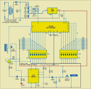
The circuit uses timer NE555 (IC2) wired as a monostable. When push-to-on switch S1 is pressed, IC2 generates a 50ms pulse, which is given to the program pin 18 of the ZIF SOCKET through switch S2. EPROM is inserted into the ZIF SOCKET for programming. LED1 glows to indicate the application of the programming pulse to the EPROM. Before applying the programming pulse to the EPROM, select the programming voltage (25V, 21V or 12.5V, as specified by the manufacturer) applied to pin 21 of the ZIF SOCKET by using jumper J1. The programming voltage required for an EPROM is sometimes written on its body. The address and data for the EPROM (ZIF SOCKET) are set by using DIP switches SW1 and SW2, respectively, whose pins are initially pulled high via 10-kilo-ohm resistors.
The AC mains is stepped down by transformer X1 to deliver 30V, 250 mA from the secondary. The secondary output is rectified by diode D1 and filtered by capacitor C1. The programming voltages of 25V, 21V and 12.5V are generated with the help of zener diodes ZD1, ZD2 and ZD3. IC1 is used to provide +5V regulated supply to the circuit.
To begin with, first read the programming voltage written on the EPROM. Now insert the EPROM chip into the 24-pin ZIF socket and slide switch S2 as per EPROM. Then connect the power supply to provide regulated 5V DC to the circuit. Select the programming voltage using jumper J1 and set the programming address and data value using switches SW1 and SW2, respectively. After providing the required programming voltage, press switch S1 to program the data at the desired address. Repeat this procedure for the next address and corresponding data.
Manual Eprom Programmer Circuit Diagram

The circuit uses timer NE555 (IC2) wired as a monostable. When push-to-on switch S1 is pressed, IC2 generates a 50ms pulse, which is given to the program pin 18 of the ZIF SOCKET through switch S2. EPROM is inserted into the ZIF SOCKET for programming. LED1 glows to indicate the application of the programming pulse to the EPROM. Before applying the programming pulse to the EPROM, select the programming voltage (25V, 21V or 12.5V, as specified by the manufacturer) applied to pin 21 of the ZIF SOCKET by using jumper J1. The programming voltage required for an EPROM is sometimes written on its body. The address and data for the EPROM (ZIF SOCKET) are set by using DIP switches SW1 and SW2, respectively, whose pins are initially pulled high via 10-kilo-ohm resistors.
The AC mains is stepped down by transformer X1 to deliver 30V, 250 mA from the secondary. The secondary output is rectified by diode D1 and filtered by capacitor C1. The programming voltages of 25V, 21V and 12.5V are generated with the help of zener diodes ZD1, ZD2 and ZD3. IC1 is used to provide +5V regulated supply to the circuit.
To begin with, first read the programming voltage written on the EPROM. Now insert the EPROM chip into the 24-pin ZIF socket and slide switch S2 as per EPROM. Then connect the power supply to provide regulated 5V DC to the circuit. Select the programming voltage using jumper J1 and set the programming address and data value using switches SW1 and SW2, respectively. After providing the required programming voltage, press switch S1 to program the data at the desired address. Repeat this procedure for the next address and corresponding data.
Sourced By: EFY Author: Priyank Mudgal


